Table of Contents
Central Processing Unit
a display of not-so-black boxes
By: Lyra Silverwolf
What I Did
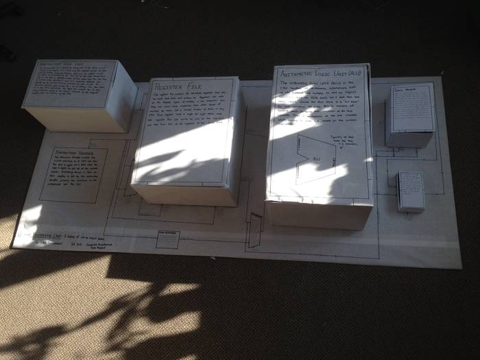
I built a display/diorama of an entire computer Central Processing Unit (CPU) out of nested cardboard boxes.
At the highest level of abstraction are the 5 major information stages a CPU is commonly divided into: instruction fetching, instruction decoding, the register file, the arithmetic logic unit (ALU), and data memory. I chose these particular stages for the CPU, because in a pipeline CPU when multiple instructions can be executed simultaneously, these are the typical partitions.
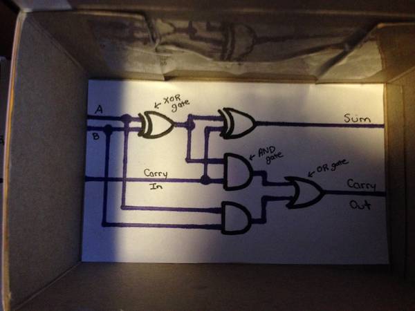
Inside of each outer level box are more boxes representing what happens inside of that particular unit. For example, inside of the ALU there is a box for the adder/subtractor, which in turn contains a box with a gate level schematic of a 1-bit full adder inside. This allows the person exploring the diorama to extrapolate how the components fit together all the way from the individual gates to the top-level information stages.
Why I Did It
There were several reasons I chose to make a physical display of a CPU for my final project. First of all, I think that Computer Architecture is a very exciting field, and I wanted to make it more approachable for all audiences. When I set out to construct this display I had my 12-year-old sister in mind as my potential audience, and while I may have not achieved quite that level of clarity, I believe that I've made something that other Oliners can interact with and get excited about.
This project also wraps up the big picture of the entire course very well, because I've explored all of the levels of abstraction that we discussed in class throughout the semester. We started out initially talking about logic gates and binary math, and then slowly progressed up to the CPU itself, and in this project I present a little bit of everything. Through pulling it all together in this way, I certainly reinforced most of the concepts that I was having trouble with in the class and found gaps in my knowledge that I wasn't even aware I had.
How I Did It
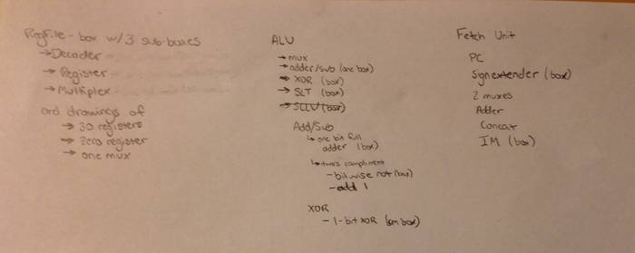
I started out by sketching out the CPU at its highest level of abstraction and deciding how many very large boxes I needed to acquire. I then determined what exactly went into each upper-level box and what subset of those things I wanted to also give boxes to.
Then I got a ton of boxes and some art supplies.
In the end I decided on the following boxes:
- CPU (more of a flat panel to put everything else on top of)
- Instruction Fetch Unit
- Sign Extender
- Instruction Memory
- Register File
- Decoder
- Single Register
- Arithmetic Logic Unit
- Adder/Subtractor
- One-bit Full Adder
- Data Memory
- One Small Multiplexer
On the lid of each box I described the function of that particular box in the context of the level within which it was contained. Inside of the box I drew a complete schematic of that item, and I wrote detailed descriptions of what each element in the schematic was responsible for doing, even if that element didn't have its own box.
Component Descriptions
The names of all the components are underlined and the components that are represented by boxes are also bolded.
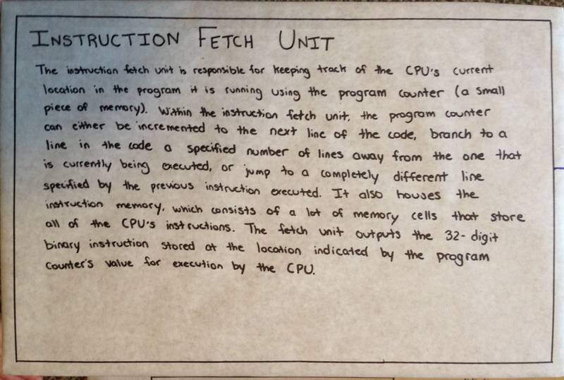
Instruction Fetch Unit - The instruction fetch unit is responsible for keeping track of the CPU’s current location in the program it is running using the program counter (a piece of memory). Within the instruction fetch unit, the program counter can either be incremented to the next line of the code, branch to a line in the code a certain number of lines away from the one it is currently on, or jump to a completely different line specified by the previous instruction executed. It also houses the instruction memory, which consists of a lot of memory cells that store all of the CPU’s instructions. The fetch unit outputs the instruction stored at the location indicated by the program counter for execution by the CPU.
Program Counter - The program counter is a register (small bit of memory) that “bookmark’s” the computer’s place in its instruction sequence so that it will know which instruction to execute next.
Concatenator - The concatenator combines the 4 highest order digits of the current program counter value with the last 26 digits of the previous instruction to build a new program counter value.
Branch Multiplexer - This multiplexer controls what is passed in as the second operand of the adder. If there is no branch and the program counter should continue on to the next operation in the instruction set, this multiplexer will pass through the zero from the top. However, the multiplexer will choose the sign-extended version of the immediate value passed in through the previous instruction if the program counter should branch to a different part in the code a certain number of lines ahead.
Adder - The adder either adds only 1, using the carry-in, or the sign-extended immediate value and 1 to the previous program counter value depending on the output of the branch multiplexer.
Jump Multiplexer - This multiplexer has the final say over what the next program counter value will be. It either chooses the output of the concatenator if a jump is specified or the output of the adder if the program counter will be continuing or branching. The blue “jump” input at the bottom chooses which data is passed through.
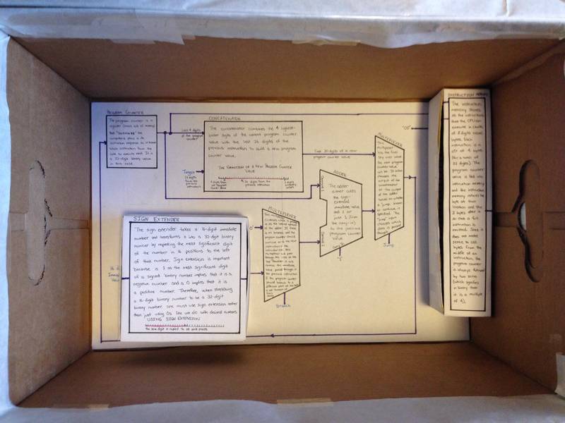
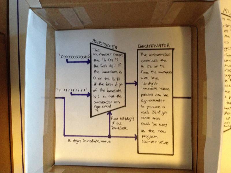
Sign Extender - The sign extender takes a 16-digit immediate number and transforms it into a 32-digit binary number by repeating the most significant digit of the number in 16 positions to the left of that number. Sign extension is important because a 1 as the most significant digit of a signed binary number implies that it is a negative number and a 0 as the most significant digit implies a positive number. Therefore, when stretching a 16-digit binary number to be a 32-digit binary number, one must use sign extension rather than just using 0’s like we do with decimal values.

Sign Extender Multiplexer - This multiplexer chooses 16 0’s if the first digit of the immediate is 0 or 16 1’s if the first digit of the immediate is 1 so that the concatenator can sign extend the immediate.
Sign Extender Concatenator - The concatenator combines the 16 0’s or 1’s from the multiplexer with the 16-digit immediate value passed into the sign extender to produce a valid 32-digit value that could be used as the program counter value.
Instruction Memory - The instruction memory stores all of the instructions that the CPU can execute in chunks of 8 digits called bytes. Each instruction is a set of 4 bytes (for a total of 32 digits). The program counter value is fed into the instruction memory, and the instruction memory returns the byte of information at that location and the 3 bytes after it so that a full instruction is emitted. Since it does not make sense to call bytes from the middle of an instruction, the program counter will always end in two zeros (which signifies in binary that it is a multiple of 4).


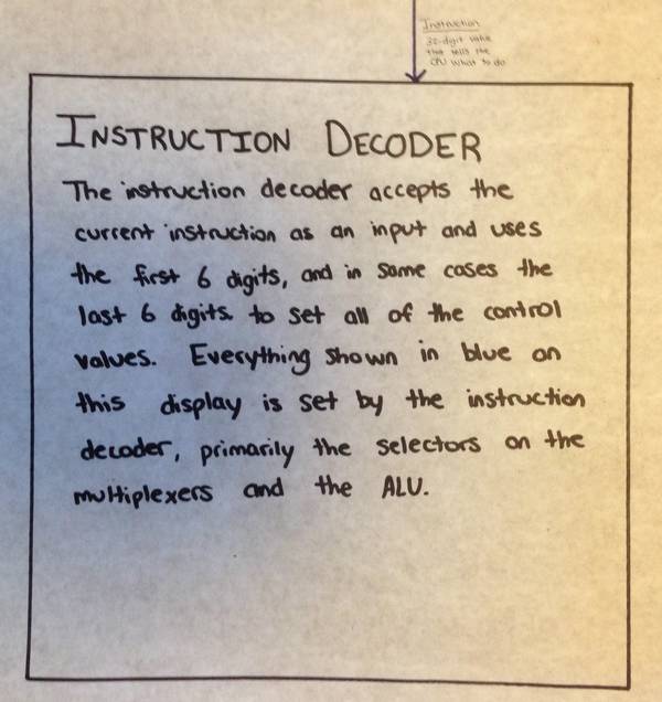
Instruction Decoder - The instruction decoder accepts the current instruction and uses the first 6 digits and in some cases the last 6 digits to set all of the control values for the multiplexers and the ALU (everything shown in blue in this display).
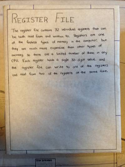
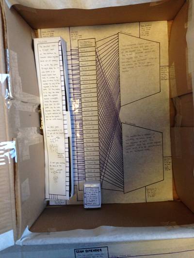
Register File - The register file contains 32 individual registers that can be both read and written. Registers are one of the fastest types of memory in the computer, but they are much more expensive than other types of memory, so there are a limited number of them in any CPU. Each register holds a single 32-digit value, and the register file can write to one of the registers and read two of the registers at the same time.
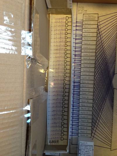
Decoder - The decoder uses a 5-digit input at the bottom to choose which register (small bit of memory) to write the given 32-digit data value to. It also takes in an enable signal that tells it whether to allow a value to be written to any of the registers in the first place. If this enable is 0, then the data inside of the registers remains unchanged. Inside of the decoder, there are 32 AND gates, one for each register, that take 6 inputs each (one of each of the signals and the write enable). An AND gate only outputs a “1” if all of its inputs are 1’s.

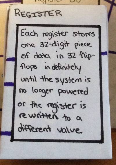
Single Register - Each register stores one 32-digit piece of data indefinitely until the system is no longer powered or the register is rewritten to a different value.

Multiplexer 1: This multiplexer chooses which registers to read from the register file. Based on the 5-digit selector passed into the register file, the multiplexer chooses and outputs the 32-digit data stored in the corresponding register.
Multiplexer 2: The register file is capable of outputting the values stored in two registers at once. This multiplexer reads that second register to output, exactly like the multiplexer above.
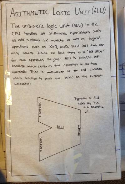
Arithmetic Logic Unit - The arithmetic logic unit (ALU) in the CPU handles all arithmetic operations such as add, subtract and multiply as well as logical operations such as bit-wise XOR, AND, NOT, set if less than, and many others. Inside the ALU, there is a “bit slice” for each operation the given ALU is capable of handling, which performs that operation on the two operands. Then a multiplexer at the end that chooses which solution to pass out, based on the current instruction.
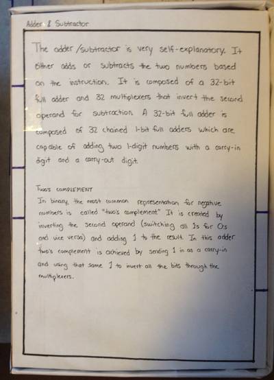
Adder/Subtractor - The adder/ subtractor is very self-explanatory. It either adds or subtracts the two numbers based on the instruction. It is composed of a box that converts a positive number to a negative number (for the subtraction) and a 32-bit full adder. A 32-bit full adder is composed of 32 chained 1-bit full adders which are capable of adding two 1 digit numbers with a carried in digit and a carried out digit. In binary, the most common negative representation used is called the “two’s complement” and it is created by inverting each of the bits and then adding 1.
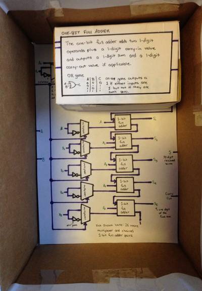
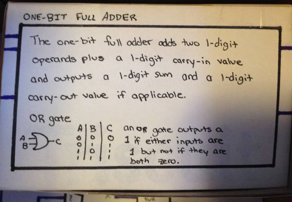
One-bit Full Adder - The 1-bit full adder adds two 1-digit operands plus a 1-digit carry-in value and outputs a 1 digit sum and a 1-digit carry-out value if applicable.
XOR - Exclusive OR (XOR) is a bitwise-logical operation performed by the ALU that examines each pair of digits in the two operands starting with the least significant digit of each. If the two compared digits are different, the digit in that place of the output is a 1. If the two compared digits in the operands are the same, then the corresponding digit of the output is a 0.
SLT - Set if less than returns a 1 if the second value is less than the first and a zero if not. It determines which number is larger by subtracting the two values and examining the sign of the subtractor’s output. Negative binary numbers always start with 1 and positive numbers start with 0.
SLLV - The shift left logical variable shifts the whole string left by a power of 2 places specified by the instruction. Then the spots on the right left empty are filled with zeros, which in binary is effectively multiplying the number by two to the power of the number of places it is shifted left.
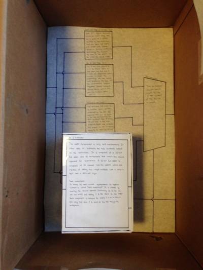
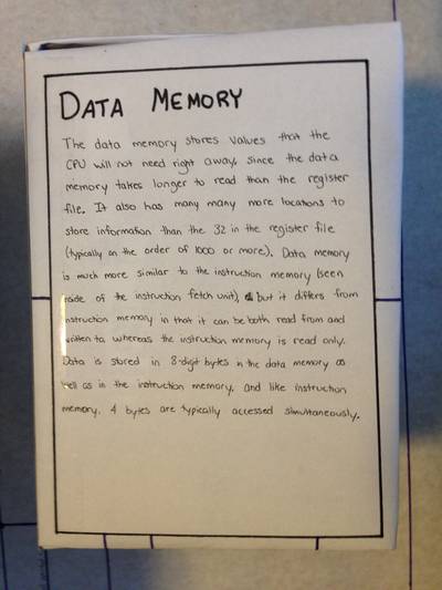
Data Memory - The data memory stores values that the CPU will not need right away, since the data memory takes longer to read than the register file. It also has many many more locations to store information than the 32 in the register file (typically on the order of 1000 or more). Data memory is much more similar to the instruction memory (seen inside of the instruction fetch unit) differs from instruction memory in that it can be both read from and written to, whereas the instruction memory is read only. Data is stored in 8-digit bytes in the data memory as well as in the instruction memory, but like instruction memory, 4 bytes are typically accessed simultaneously.
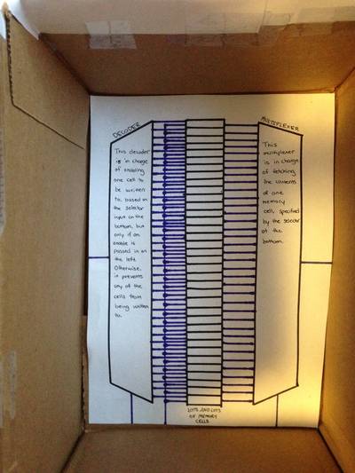
Decoder: This decoder is in charge of enabling one cell to be written to based on the selector input at the bottom if an enable is passed in on the left. Otherwise, it prevents any of the cells from being written to.
Multiplexer: This multiplexer is in charge of fetching the contents of one cell, specified by the selector at the bottom.
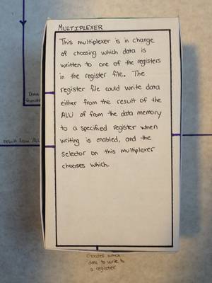
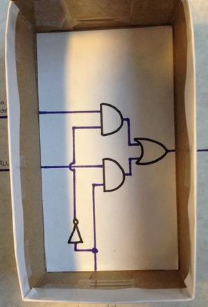
Data to Register Multiplexer - This multiplexer is in charge of choosing which data is written to a register in the register file. The register file could write data either from the result of the ALU or from data memory to a specified register depending on the selector, and this multiplexer chooses which of those to do.
Future Work
In the end I wound up with a CPU that I could show off to a fellow Olin student, but I don't think that my 7th grade sister would understand it without me explaining it to her. If I were to continue to build on this project, I would make everything bigger so that I could add more detail everywhere to widen the audience. I was severely constrained by the sizes of the boxes I had access to, which made it hard for me to nest multiple boxes inside of one another and add an appropriate level of detail to the project.
I also would like to include a reference packet that discusses the things I didn't have room to outline on the display like the logic gates and how a multiplexer or decoder uses the selector wires to select which input or output to use.
'Gotchas'
The main gotcha in this project was cutting the paper. Drawing the schematics took a long time, but it took an even longer time to cut the paper and cover everything to make it look pretty. It was also difficult to determine what level of detail I should portray on each level of abstraction.
Work Plan
Goal
To create a physical display that explains what a CPU does and how it works. There will be several nested black boxes (IRL) and each one will be labeled with a description explaining what goes on inside of that black box. The largest box will be the CPU as a whole and the smallest black boxes will be the simple gates. The audience for these descriptions will be a parent or sibling that doesn’t know anything about computer architecture.
I would also like to show some simple operations taking place in the CPU, preferably user-controlled. I could have a knob or series of buttons that activated a different set of lights through the display depending on the operation, or it could be as simple as using different colors of yarn for different operations with careful labeling.
Final demo
The above display with a short presentation that I could give at expo explaining what a CPU is and why Computer Architecture is so cool.
Rough Schedule
Wednesday Dec 4th - Have “schematic” of entire system, begin procuring boxes (2 hours)
Saturday Dec 7th - Decide which operations will be shown and how (1 hour)
Sunday Dec 8th - Have all descriptions completely written (5 hours)
Wednesday Dec 11th - Assemble the display (4 hours)
Saturday Dec 14th - Finishing assembling the display/ wire lights(?) (2 hours)
Sunday Dec 15th - Presentation complete (1 hour)
Sunday Dec 15th - Documentation complete (5 hours)
Monday Dec 16th - Project due
Work Plan Reflection
I massively mis-judged this project. Not only did I want to include all of the possible detail on every level of abstraction, but I also wanted to have non-trivial user control over information flow, both of which turned out to be harder than they seemed.
As far as the schedule goes, the order I laid out for myself did not end up to be effective either. I did come up with the schematic first, but the rest was dictated by the boxes that I had available to me, so I built the project module-by-module rather than writing all the descriptions and then putting them on the boxes. I also mis-judged how long it would take to assemble something of this scale, so instead of taking 4 hours to put it all together, it took me at least 20 total. Therefore, I was unable to implement the user-controlled data path following through the system.
I also did not judge how far apart Monday and Thursday are in finals week, so instead of having my whole project done by Monday, I only had 1.5 modules done by that point. Therefore, I was unable to give the type of presentation that I had anticipated giving during the final block for CompArch.
I did implement a basic version of what I had planned to do, and I did learn a lot doing it, so overall I'd call my project a success. I was just not super accurate in my original work plan.
