Table of Contents
Project Pineapple: Cats on Screens
LCD Driver on an FPGA
Steph "Grape" Northway
Dimitar "Orange" Dimitrov
Due December 16, 2014
We implemented a driver for the LCD screen in Figure 1, a 1.8 inch color display. Our implementation stores a photograph of a kitten in memory, initializes the screen, and writes the picture to the screen (in color!).
Why? We love to look at cats. Actually though, it was because VanWyk said itwas a hard project and we wanted to do a hard project. It was also a good project to scaffold for future work (i.e. our basic goals of writing a picture to the screen feed into cooler goals of reading from a camera very nicely).
Our general approach was to figure out and test the low-level controls for the screen with an Arduino and then design a circuit in Verilog to carry them out.
Arduino Simulation
If you Google our screen, the ST7753 1.8“ TFT SPI display, you will quickly find Lady Ada's guide. However, short of a brief intro, it achieves little in uncovering how the display is controlled. It does link to the datasheet for the display's chip, but this 164-page document is useful for little but reference.
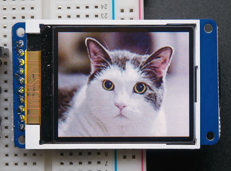 |
| Figure 1: CATS (not our cat, though) |
However, you may download Adafruit's two libraries for this chip, as well as some example code. Parsing the C++ reveals the following about screen control:
1. All signals sent are over SPI (duh). The screen returns nothing over MISO (0xFF, actually) in the default configuration.
2. There are two types of SPI signals that could be sent: “Command” and “Data”. The type is determined on the D/C input pin.
3. Command signals determine the meaning of the Data signals following (for instance, the signal 0x2C, aliased as ST7735_RAMWR, means the following data will correspond to pixel colors, which we will discuss soon).
4. At least 21 different commands (with data following) need to be sent every time the screen is powered on to configure it. Some are more opaque than others, even for Ada Lovelace herself:
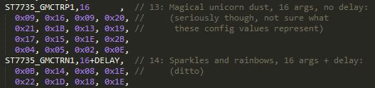 |
| Figure 2: Highlights from the Adafruit library code |
5. There are about 6 different combinations of these in Adafruit's library alone based on which version of the screen you have. For ours, it was the Rcmd1, Rcmd2red and Rcmd3 sets.
6. To complicate matters further, some commands require a delay time after they're executed.
7. After initialization, there are three important commands:
- 0x2A (ST7735_CASET), which sets the start and end x-coordinates of the drawing field
- 0x2B (ST7735_RASET), which sets the start and end y-coordinates of the drawing field
- 0x2C (ST7735_RAMWR), which sets the pixel colors in the drawing field.
8. Colors are represented in two bytes according to the following diagram (from the huge datasheet):
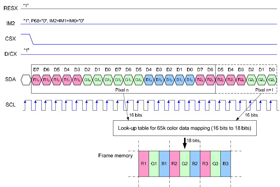 |
| Figure 3: Of course, this is one of MANY options set by 0x3A (ST7735_COLMOD). |
9. They are placed in consecutive order starting from the left-hand top-most pixel in the drawing area. Here's an example.
10. The screen isn't very fast. Timing needs to be slow enough, otherwise the screen does not react.
Given this information, we wrote an Arduino script using the SPI signals we would send from the FPGA.
The original code had a complicated way of keeping track of the D/C selector pin, using nested counting which would have proven difficult and wasteful to implement in Verilog. Instead, we modified the 8-bit signals, adding two bits in front of each as op-codes:
- 0x0XX indicates that the signal is Data (thus the D/C pin must be HIGH when it's sent)
- 0x1XX indicates that the signal is Command (D/C LOW)
- 0x2XX indicates it is a delay
We used this encoding in both our Arduino simulation and our final Verilog. The Arduino simulation had an additional 0x300 code signifying the end of a group of signals, allowing us to iterate groups of signals and conserve space. The code for this last bit was largely inspired by code found in Adafruit's library.
Here is the full simulation code, including initialization instructions for our display, three sample color groups and sample functions iterating them. This code does not use the Adafruit library at all, and it doesn't use the Arduino SPI library (and the ATMega's hardware SPI). Instead, it manually controls SCLK, MOSI, CS, D/C and RST (used only to activate the board initially). Here's a video of these examples in action.
Unfortunately, the ATMega is too Tiny to store even a kitten (the cat above lives on an SD Card - lame!). Given more space, a list of colors (which can be extracted and converted to the correct format from any jpeg using this python script) could simply be inserted as a group and displayed using
commandList(Kitteh)
.
Verilog Implementation
After we had figured out how to write individual pixels with the Arduino, we started designing the architecture of our Verilog implementation. It ended up being very similar to that of the SPI lab, for obvious reasons; we used code from the lab for our shift register, with some parameter changes. Below is the block diagram of the system, where blue indicates inputs and red indicates outputs:
 |
| Figure 4: Block diagram of Verilog implementation |
The following sections discuss the functions of each block.
Serial Clock
The serial clock module replaced the switch-driven serial clock from the SPI lab. It takes the system clock as its only input and divides its frequency by a power of 2 to get the SCLK output. The positive and negative edges of SCLK are also outputs for use in various other components. The last output is “SCLK/8”, which is a signal that goes high for one clock cycle (of the system clock) every eight SCLK cycles.
Shift Register
This is very similar to the shift register from the SPI lab, with some simplifications. It takes in 8 bits of parallel data when Enable is high; Enable is only high every 8 serial clock cycles, preventing new bytes from being read in before the previous one is done being read out through the serial output pin.
Program Memory
This is by far the largest part of the design. The screen is 160×128, which is 20480 pixels total; since each pixel is 2 bytes that makes for a program memory depth of 40960, not even counting the initialization commands, just to store a cat picture. We implemented this by generating the hexadecimal strings in a text file with Python, saving them in a .dat file, and using $readmemh to populate the memory in Verilog. Extra information is appended to the bytes in the form of 2-bit op codes at the beginning of each byte, for a width of 10. The program memory takes in the address (16 bits wide, as ceil(log2(40960))=16) of the byte and outputs the op code to the instruction decoder and the data to the shift register.
Instruction Decoder
We first tried to implement this as an FSM, but soon realized we actually needed an instruction decoder. There are 3 instructions: write data, write command, and delay. The instruction decoder outputs the chip select (high for delay instructions), the data/command select, and an enable to the delay counter.
Delay Counter
When the instruction is delay, the delay counter gets a signal to start. The Adafruit code had several different delay times for different commands, but we found that making them all the same had no effect on the screen's ability to display images, so the delay is fixed in the Verilog code. While the delay is happening, the program counter is disabled by the low PCEn output. When the delay signal from the instruction decoder is low, the signal is high and the program counter can proceed as usual.
Program Counter
This program counter increments by 1 every eight serial clock cycles unless disabled by the delay counter module. It outputs the 16-bit address of the current byte in memory.
MISO Flip Floop
This is just a regular D flip flop to synchronize the output of the shift register to the negative edge of the serial clock, which is expected with SPI. Its output is the MOSI input to the LCD screen.
Lessons Learned
Though both team members are very happy with this project and feel like we learned a lot doing it, there are several things we could have done better. For example, we didn't end up getting the Verilog on an FPGA in time for class demos because between every permutation of 3 computers and 2 FPGAs none of them could connect correctly when performing the boundary scan. Had we tried the FPGA earlier we could have overcome that roadblock, but we just sort of assumed it would work.
Another thing that tripped us up a bit was the issue of timing in Verilog. For an LCD screen to work, the timing has to be exactly correct or nothing will look right. We had several instances of signals happening one clock cycle off from other signals, and this was because we used always *@(posedge clk)” for almost every module initially. The solution to this was usually either “always @(*)” or using the edge of one of the other timing signals.
Finishing the Job
The first step for anyone trying to pick up the pieces would be to try to put this on an FPGA. All the
Verilog (complete with Cat) is on GitHub (see bottom of page) as well as in this ZIP file. To build, they should be imported into a new ISE project. There is also a working project on GitHub under /strawberry. If more testing is necessary, a few Arduino simulations are also on GitHub, under /ArduinoTests. Code for image conversion can be found under /images. The screen needs to be connected the the FPGA as follows:
LITE → External 5V supply with common GND
MISO → N/A
SCK → gpioBank1[3]
MOSI→ gpioBank1[0]
TFT_CS → gpioBank1[1]
SD_CS → N/A
D/C → gpioBank1[2]
RESET → gpioBank2[0]
VCC → External 5V supply with common GND
GND → GND
The next step we intended for this project was attaching a camera to the FPGA and streaming pictures and/or video to the screen. The camera we researched is the OV7670. This seems to be a good starting point.
We're on GitHub! - https://github.com/dimitdim/pineapple