Snap Circuits
For questions, please contact Nicole.Rifkin@students.olin.edu or Mitchell.Cieminski@students.olin.edu
LOGIC GATES:
Logic gates take in some number of inputs, where each input is a binary value: a true input is represented with a 1, and means that some voltage is supplied. A false input is represented with a 0, and means that there is no voltage supplied. Logic gates always have an output that is dependent on the inputs. A logic gate’s behavior is represented with a truth table, which describes each output for every combination of inputs. The first columns are the inputs, and the last column is the outputs. This can best be understood by example.
SNAP CIRCUITS:
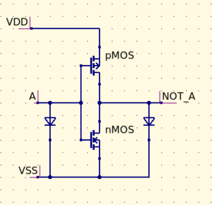
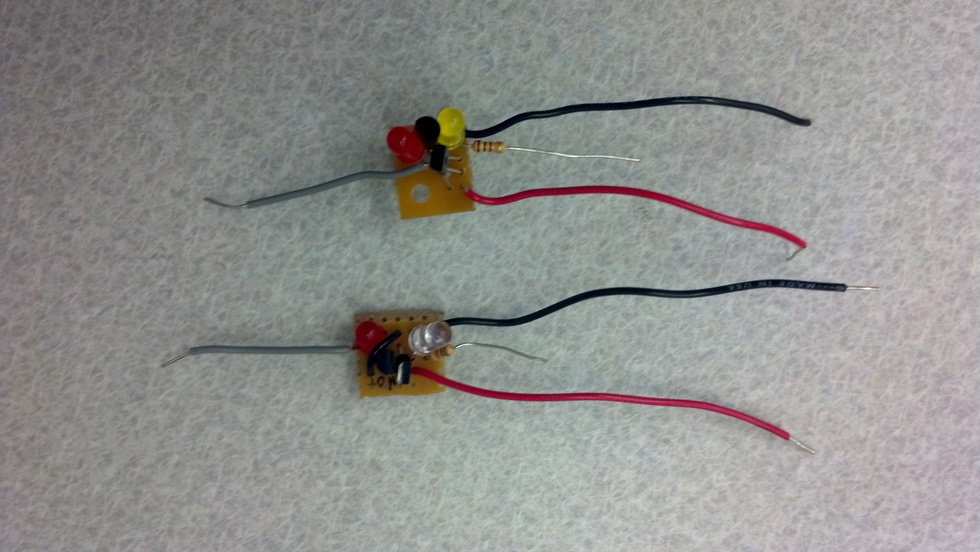
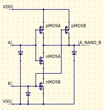
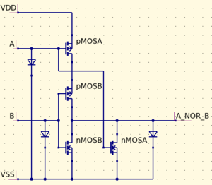
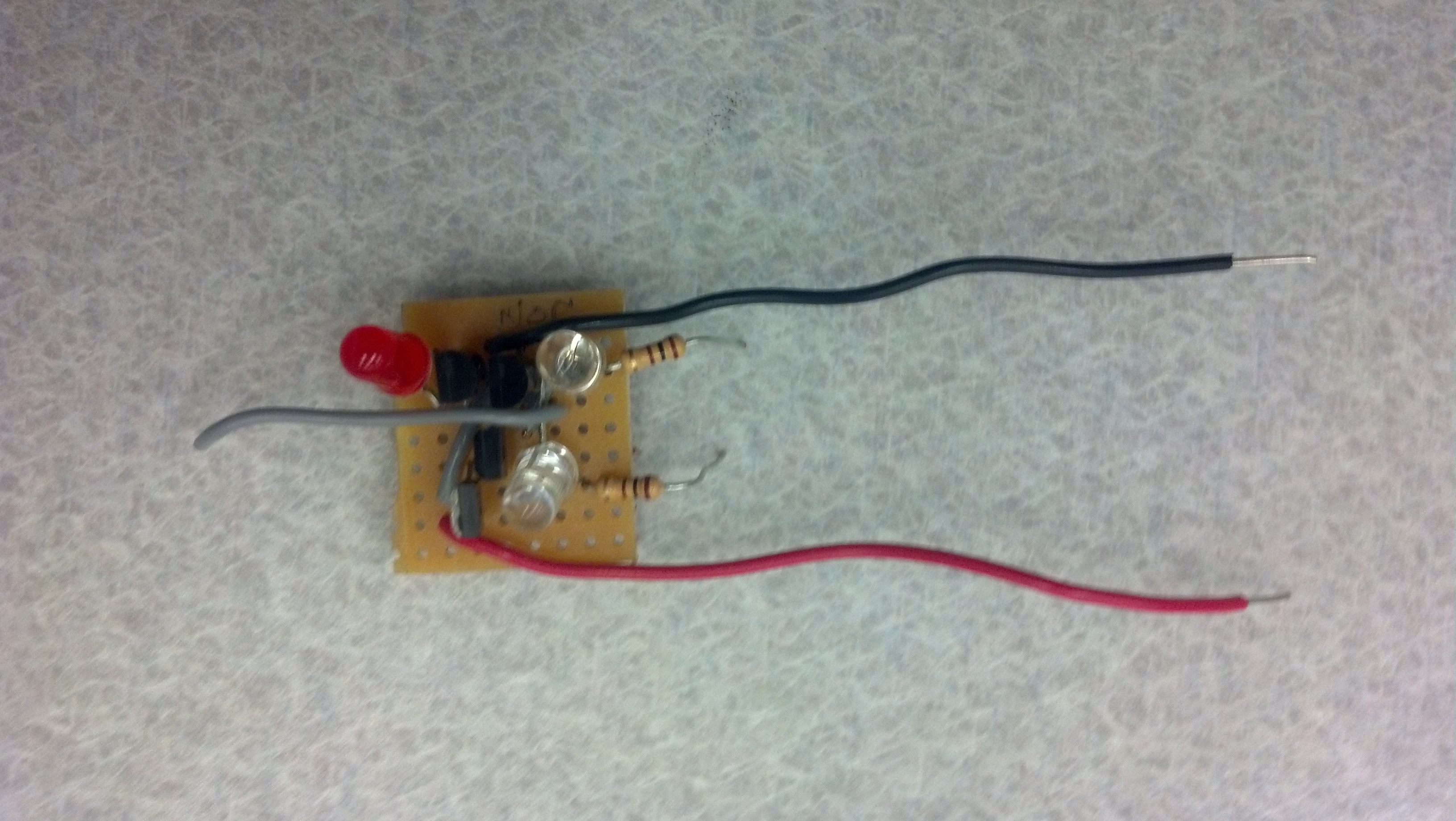
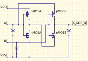
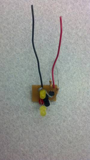
Snap circuits were built using transistors to create physical representations of basic logic gates. Each snap circuit gate contains green or yellow LEDs for the inputs and red LEDs for the outputs, and is designed to make logic interactive and easy to visualize. The schematics of the design are included in the lesson plan. You can build your own Snap Circuits at home by purchasing solder prototyping boards or breadboards, mosfet transistors, and LEDs and building the circuit schematics pictured below.
NOT:
An inverter or not gate takes a single input and outputs the opposite. The truth table looks like this:
| INPUT | OUTPUT |
|---|---|
| 1 | 0 |
| 0 | 1 |
The input column shows what you give it, and the output column shows what it gives you.
The snap circuits kit comes with multiple NOT gates, because they're quite important.
AND:
An And gate’s output is true only when both input A and input B are true. Otherwise it is false. The truth table looks like this:
| INPUT A | INPUT B | OUTPUT |
|---|---|---|
| 0 | 0 | 0 |
| 0 | 1 | 0 |
| 1 | 0 | 0 |
| 1 | 1 | 1 |
You will notice that your snap circuit set does not come with an And gate, but rather a Nand gate. This is because in a computer, And gates are often constructed using a Nand gate and a Not gate. You can see a demonstration of this particular mini-project here.
NAND:
A Nand gate is the exact opposite of an And, and means Not Input 1 and Input 2. Therefore, a Nand gate has a true output except for when Input 1 and Input 2 are both true. It is very easy to create the truth table for Nand, because we already have the truth table for And. In the output column, whenever And has a 0, Nand has a 1, and vice versa. The input columns stay the same.
| INPUT A | INPUT B | OUTPUT |
|---|---|---|
| 0 | 0 | 1 |
| 0 | 1 | 1 |
| 1 | 0 | 1 |
| 1 | 1 | 0 |
If we compare And and Nand, we see:
| INPUT A | INPUT B | A AND B | A NAND B |
|---|---|---|---|
| 0 | 0 | 0 | 1 |
| 0 | 1 | 0 | 1 |
| 1 | 0 | 0 | 1 |
| 1 | 1 | 1 | 0 |
OR:
An Or gate’s output is true whenever either Input A or Input B are true. It is still true if both inputs are true. The truth table is below:
| INPUT A | INPUT B | OUTPUT |
|---|---|---|
| 0 | 0 | 0 |
| 0 | 1 | 1 |
| 1 | 0 | 1 |
| 1 | 1 | 1 |
Again, the snap circuit kit only includes a Nor. You can build an Or gate by wiring the output of the Nor gate to the input of the Not gate, just like you can for Nand/And. Try it! The output of the Not gate will be the same as the output of an Or.
NOR:
Nor is the opposite of Or, and the output is true when neither Input A nor Input B are true. Here is the truth table comparing Or and Nor. The output of the Nor truth table has a 1 wherever Or has a 0, and vice versa.
| INPUT A | INPUT B | OUTPUT |
|---|---|---|
| 0 | 0 | 1 |
| 0 | 1 | 0 |
| 1 | 0 | 0 |
| 1 | 1 | 0 |
XOR:
Xor is an exclusive Or gate. It is almost the same as an Or gate, except the output is false when Input A and Input B are both true. This means that in order for the output to be true, Input A and Input B are mutually exclusive. The truth table is as follows:
| INPUT A | INPUT B | OUTPUT |
|---|---|---|
| 0 | 0 | 0 |
| 0 | 1 | 1 |
| 1 | 0 | 1 |
| 1 | 1 | 0 |
PLAYING WITH YOUR SNAP CIRCUITS:
You can start playing with your snap circuits by connecting the red wire to the positive rail (marked with a red +) and the black wire to the negative rail (marked with a blue -) on the breadboard. Connect the positive end of a battery to the same positive rail, and the negative end of a battery to the negative rail. Place the output wire in the designated spot next to the buffer. You can now use jumper wires to send true (+) or false (-) logic to your gates. You can watch the red output to see how your gate behaves. To continue exploring, try connecting the outputs of one gate to the inputs of another. You can use our tutorials to create more advanced circuits, or explore new combinations of gates and create your own.
HALF ADDER:
You can make a one-bit binary adder out of snap circuits. This logic system has two input numbers to be added together. These are 1 if they are true logic and 0 if they are false logic. It also has a carry out, or a remainder. The LED can only be high or low, one or zero; there is no way to represent a sum of 2. Instead, we say that the sum is zero with a carry out of 1. The carry out represents the next binary digit. If you are familiar with binary, you will realize that 10 is 2 in binary. The truth table is below:
| INPUT A | INPUT B | CARRY OUT | SUM |
|---|---|---|---|
| 0 | 0 | 0 | 0 + 0 = 0 |
| 0 | 1 | 0 | 1 + 0 = 1 |
| 1 | 0 | 0 | 0 + 1 = 1 |
| 1 | 1 | 1 | 1 + 1 = 0 |
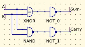
You might notice that the Carry out column looks identical to an And truth table. Similarly, the Sum column looks identical to an Xor truth table. We can build a half adder using an And and an Xor gate. You can follow the diagram or the explanation below. Connect the output of Nand and the input of Not. Use a jumper cable to connect the first input of Nand and the first input of Xor. Use a second jumper cable to connect the second inputs of Nand and Xor. Give both inputs any combination of signals you desire. The output of Not will be the carry out of your adder, and the output of Xor will be the sum of your adder. As you may have realized, what you have just built is a half adder. A full adder has three inputs. 2 are meant to be added, and a third is a carry in. This input is always wired to the carry out of the adder before it. By putting 4 full adders, one after another, you can add a 4 bit binary number.
You can see an example of the half-adder project here.
SR LATCH:
In logic, sometimes it is important to know the output of a gate as well as its last output. A latch is used to hold state, meaning that it will remember whether a value was high or low until it is reset. A Set Reset (SR) latch is a simple example. The two inputs are referred to as S and R, and it is important to know the value of the last outputs. The two outputs are unique in that one will always be the opposite of the other. The truth table will help to clarify the behavior of an SR latch. It looks like this:
| SET | RESET | Q LAST | Q | NOT Q |
|---|---|---|---|---|
| 0 | 0 | 0 | 1 | 1 |
| 0 | 1 | 1 | 1 | 1 |
| 1 | 0 | 0 | 1 | 0 |
| 1 | 1 | 1 | 1 | 0 |
| 0 | 0 | 0 | 0 | 1 |
| 0 | 1 | 1 | 0 | 1 |
| 1 | 0 | 0 | 0 | 1 |
| 1 | 1 | 1 | 1 | 0 |
A simplified version of this is:
| SET | RESET | Q |
|---|---|---|
| 0 | 0 | Latch breaks, this combination is not allowed |
| 0 | 1 | 1 |
| 1 | 0 | 0 |
| 1 | 1 | Q last |
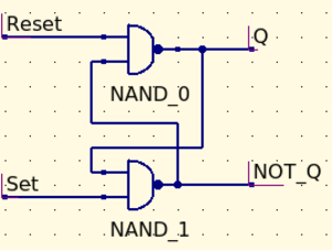
When both inputs are wired high, Q does not change until one of the outputs changes. This is useful for creating memory in a logic circuit. You can build an SR latch by using two Nand gates and wiring the output of one to the input of the other using a jumper cable. See diagram. Experiment with all inputs, and notice what happens when both set and reset are zero!
DECODER:
A decoder is used to select which output to send an input. It includes at least one selector, an input, and at least two outputs. The truth table is shows:
| SELECTOR | INPUT | OUTPUT 0 | OUTPUT 1 |
|---|---|---|---|
| 0 | 0 | 0 | 0 |
| 0 | 1 | 1 | 0 |
| 1 | 0 | 0 | 0 |
| 1 | 1 | 0 | 1 |
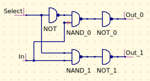
As you can see, if the input is zero, the output will always be zero. If the input is one, the selector determines which output is also one. This is useful for sending information only to the specific place that it is needed. You build it by creating two And gates, with a Not gate in front of one of them. The selector input should get wired to both the first Not gate and the And gate. The data input should be wired to both And gates. The diagram below shows this visually. See if you can predict which red LED will light up!
PERSONAL REFLECTIONS:
One of the biggest challenges of this project was thinking about ways to make it user friendly and accessible to others. I think in a lot of ways we succeeded in making a toy that is tangible and can visually show the behavior of logic circuits. However, they are not safe for children to use because there are so many exposed wires, even though it would be a great resource for them. In addition, there is a bit of a learning curve that goes along with them; it requires knowledge of how a breadboard works, and is only intuitive if you are familiar with electrical conventions, such as red wires getting power and black wires getting grounded. It was also very difficult to put together a manual that contained enough information to be useful but not so much to become a textbook. For example, currently, it puts a black box around the binary number system. It is still possible to use and enjoy the Snap circuits without knowledge of binary, but the user will not understand the adder as well. I could imagine that it would be intimidating or turn the user off to the user if they did not understand large parts of it, but at the same time, it would not be helpful to have 20 pages of documentation. We would really appreciate feedback on what parts of the manual were clear and intuitive and what parts were confusing or intimidating, because this was a part that we definitely struggled with. We also had a lot of debate on what features the actual snap circuits should include. We decided to go with nand gates rather than and gates because it is a more accurate representation of real logic gates in processors, and took fewer transistors to build. However, it was more of a challenge to explain them in our documentation. We discussed including an exaggerated propagation delay, but chose not to for a number of reasons. In a circuit of several logic gates, it could take several seconds to see the final output, which can be undesirable for the user. In addition, we tried to keep each circuit as small as possible, and ran out of physical space for an RC time delay. The most challenging part about this project was to go all the way back to the beginning of the semester when we were first learning this material, thinking about how we could have learned it better, and then trying to implement that.
In terms of timing, I think we had a fairly accurate prediction of the number of hours that we were going to put in to this project. We did not keep to our schedule, but had a good idea in mind of how long each step would take, and ended up finishing when we expected to. The timing reflections for every lab have definitely given us a better intuition collectively on how long an assignment will reasonably take.

