Chris Wallace Radmer van der Heyde VGA Display on a FPGA
What we did:
For our final project, we attempted to use an FPGA to send a cat photo to a monitor. This was done via a de-soldered vga port from an old monitor connected to some circuitry then to the FPGA. Because the output of the fpga is a digital signal and vga uses an analog signal, we also built a digital to analog converter, a buffer, and a voltage divider to convert the digital 8 bit signal to a voltage between 0 and .7 volts.
Why we did this:
We started this project, because we thought it would be cool to use a FPGA to display images on a screen. None of our labs this year involved interface with a video device, so we thought it would interesting to try it.
How we did it:
Our Goal Approach:
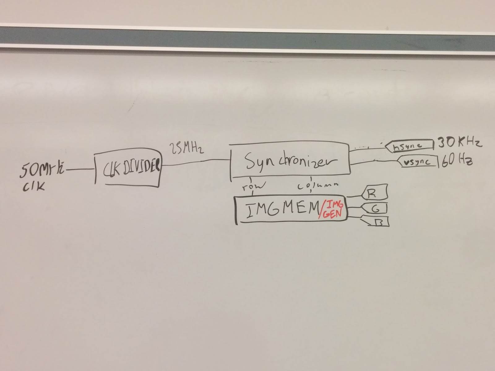
To load a image into the FPGA, we preallocated a data memory with the RGB values for each pixel in it. To obtain these pixel values, we wrote a python script that converts each 256 RGB value to hex and appends them together. FIle can be found here: writetofile.zip Each entry then, in the data Memory, is a 24 bit word with 8 bits for each value. We then wrote a module to read off the values in the memory at each pixel. We read each pixel on the positive edge of our pixel clock running at 25 MHz, and send out the each color value to the pins on the FPGA. We also produce a horizontal and vertical synchronization signal at a frequency of 31.4 kHz and 60 hz. Since VGA is an analog standard, we needed a way to convert the digital signal to an analog signal the correct way to do that is with a DAC (Digital Analog Converter). You input the bits of your digital signal and a series of voltage dividers turn that into a fixed voltage between a certain range. A schematic and good explanation can be found here: http://en.wikipedia.org/wiki/Resistor_ladder#R-2R_resistor_ladder_network_.28digital_to_analog_conversion.2C_or_DAC.29
VGA’s RGB values operate from 0-.7 volts, our DAC output a voltage between 0 and 3.3 volts, we needed to cut this down. The VGA receiver in the monitor makes this slightly easier, since it has a pulldown resistor we can form a voltage divider by putting a resistor before our VGA cable. The value that worked best for us was 260 ohms.
This waveform shows how each signal should look, the pixel clock is orders of magnitude faster than the horizontal sync, and that is orders of magnitude faster than the vertical sync. You should also notice that at the end and beginning of each sync signal the RGB values should be zero.
Reality:
However, due to many of the difficulties that we mention later, we were unable to do this. What we did instead was output a test pattern of several vertical bars on a monitor. These bars were made by combining pure RGB values, this eliminated our need for a DAC. Our RGB signal was generated within our counter, and every 80 counts (pixels) we change the value of the red green and blue signals to form a different color.
Reproduction:
In order to implement this you can follow these steps:
`1. Download our code from the wiki. finalproject.zip
2. If you are attempting to run our scaled down version where we generate a test image the relevant folder is “ScaledDownVersion” if you wish to modify the code involving a synthesized data memory the code is in “DataMemoryLoad” 3. In both directories the relevant file is “Vgatop.v” the module top can be implemented in XIlinx,most files in those directories are for test, but may be of assistance to you. 4. If attempting to implement the data memory with your own image, you must download the python script mentioned earlier and modify the data memory file such that it loads from that file. 5. Before you implement any of these, it is a good idea to read our difficulties section.
Workplan:
Due to VGA’s analog signal, we should have allocated more time than the 48 man hours we spent on the project. This is because there is a lot more to go wrong and test, and for us a large amount of time disappeared debugging the FPGA when the problem was the circuitry connecting it to the VGA port.
Block Diagram:
DIfficulties:
We experienced many difficulties in this project. The first difficulty was the time it took to synthesize onto the FPGA, in hindsight synthesizing a preallocated memory of our image was a bad idea. It would have been much better to send the data to the memory from our laptop or have chosen to make a tile of smaller images. There was also a lot of electrical issues. In the VGA standard every pin that is listed as a ground pin must actually be grounded, they do not tie together in the vga cable. It is also crucial that you send a ground signal during the “front porch” and “back porch” period, this is something we didn’t understand initially.
Future Work:
Since we struggled through the difficulty of trying to make analog video, someone else does not have to. Meaning, projects that involve video can get off of the ground faster. So, it would be easier to go from where we left off, to making a video game, or crazy video generator of some kind.


